MeesterDaan (talk | contribs) |
MeesterDaan (talk | contribs) |
||
| Line 46: | Line 46: | ||
</Center> | </Center> | ||
| − | Print #1 and Print #2 are arrangements of gates on a base, and all it takes is to wire the appropriate gates together. There are three [[Chips & Circuits - Net Lists | Net lists]] (one more in [http:// | + | Print #1 and Print #2 are arrangements of gates on a base, and all it takes is to wire the appropriate gates together. There are three [[Chips & Circuits - Net Lists | Net lists]] (one more in [http://http://heuristieken.nl/resources/CC_netlists2.txt txt-format]) for each print. Each net list needs to be implemented. The gates are numbered from left to right and from top to bottom. Nets can only follow the grid, only one wire per segment, and one step costs 1 unit length. Nets that are aligned among the same gird line are said to be in <I>conflict</I>. If there is one conflict in one arrangement, the circuit cannot be used. Nets can also go up and down to lower and higher layers, also at the cost of 1 per level. The assignment is to implement all nets in all netlists at minimum cost. |
Revision as of 23:03, 25 March 2015
Contents
Warning
Although this assignment has been simplified, it might still be quite hard.
Introduction
Chips (or more precisely: integrated circuits) are found in your PC, MacBook, Android Phone and microwave oven where they perform a diversity of functions, ranging from timekeeping and motor control to arithmetic and logic. Basically a small plate of silicon, chips are usually designed logically and subsequentially transformed to a list of connectable gates. This list, commonly known as a net list is finally transformed into a 2-dimensional design on a silicon base.
This last step however, the physical real-world process of connecting the gates, is highly volatile. Good arrangements on the base lead to short connections, leading to faster circuits, whereas poor arrangements lead to slower circuits. It leads to no doubt that a good arrangement of logical gates and good wiring between them is of vital essence to the performance of the IC as a whole.
To make things easier, we will consider the wiring problem only. The gates have already been arranged, and all it takes is finding very short wiring patterns.
Example
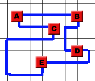
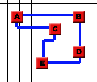
This is an integrated circuit built up from five gates that need to be connected. The connections ("nets") follow the grid in a Manhattan style. Luckily enough, the wires don't cross. Sometimes they have to and when they do, the base consists of multiple grid layers. Besides going North, South, East and West, nets can also go up and down, and the distance between levels is identical to the distance between grid points.
Assignment
Print #1 and Print #2 are arrangements of gates on a base, and all it takes is to wire the appropriate gates together. There are three Net lists (one more in txt-format) for each print. Each net list needs to be implemented. The gates are numbered from left to right and from top to bottom. Nets can only follow the grid, only one wire per segment, and one step costs 1 unit length. Nets that are aligned among the same gird line are said to be in conflict. If there is one conflict in one arrangement, the circuit cannot be used. Nets can also go up and down to lower and higher layers, also at the cost of 1 per level. The assignment is to implement all nets in all netlists at minimum cost.
A few steps to pave the way towards a program:
1) Build a computer program that holds a data structure for a grid with fixed gates.
2) Expand your program by making a data structure for a net list. Make sure it holds a few nets, and that the program calculates the total wire length.
3) Add 7 more layers. Try to get all the nets in. You can either build up wire-by-wire and step-by,step or with all wires in place, suboptimal and conflictuous, and try to improve. Whatever you do: record data to analyze for your report.
Advanced
For each of the three arrangements, try to determine the relation between the number of wires and the required number of layers.
Questions & Answers (November 2nd, 2014)
1) "only one wire per segment", does this means multiple nets can use a grid intersection?
No, it doesnt. Each grid intersection can support just one net (or "wire"). Still, this might cause problems around the logical gates, so maybe an exception should be made there. We don't know yet, as this is quite a new case.
2) The edges of the prints as shown in the pictures, can we use them to route nets, or should the nets stay clear of the edges?
Yes. You can consider the base to extend a little beyond the picture, and therefore all intersections in the picture can be used.
3) A new layer, should it be somewhere specific, or can we place it where we want?
A new (second, third, fourth) layer provides a means for your nets to go down one level. So, if you add a level to your chip, it is everywhere. But, if a layer (for instance a seventh or eight layer) is unused, it should not be placed of course, to keep manufacturing costs down.
4) Can unconnected gates be removed?
No, but I'd like to know which ones are, so I can hook them up next time to make the case look nicer.
5) Can unconnected gates be regarded "null" and may nets run through them?
No!
6) Can loose segments of several logical gates be distributed elsewhere on the base?
No. According to Simon and Robin, this is exactly what made the last version of this case too hard. So even though it's really desirable designwise, I don't want it in this version of Chips and Circuits.
Links
No links.
Bacq
Bakc to the Heuristics main page.


